Advancements in Semiconductor Manufacturing
Semiconductors are the backbone of modern technology, powering everything from smartphones to artificial intelligence systems. Over the years, advancements in semiconductor manufacturing have led to increased performance, reduced power consumption, and lower production costs. These innovations have transformed industries and paved the way for future technological breakthroughs.
One of the most significant advancements in semiconductor manufacturing is the continued miniaturization of transistors. According to Moore’s Law, the number of transistors on a chip doubles approximately every two years, leading to exponential growth in computing power. While traditional silicon-based transistors have approached their physical limits, researchers are exploring new materials and techniques such as FinFET (Fin Field-Effect Transistor) and Gate-All-Around (GAA) technology to sustain this progress.
Miniaturization and Moore’s Law
One of the most significant advancements in semiconductor manufacturing is the continued miniaturization of transistors. According to Moore’s Law, the number of transistors on a chip doubles approximately every two years, leading to exponential growth in computing power. While traditional silicon-based transistors have approached their physical limits, researchers are exploring new materials and techniques such as FinFET (Fin Field-Effect Transistor) and Gate-All-Around (GAA) technology to sustain this progress.
EUV Lithography
Extreme Ultraviolet Lithography (EUV) is a groundbreaking technology that enables the production of smaller and more efficient semiconductor components. EUV lithography uses shorter wavelengths of light to create finer patterns on silicon wafers, allowing chipmakers to manufacture transistors at the 7nm, 5nm, and even 3nm scale. This technology significantly enhances chip performance while reducing power consumption and production costs.
3D Chip Stacking and Advanced Packaging
Traditional semiconductor manufacturing relied on planar transistor arrangements, but 3D chip stacking has revolutionized the industry. Technologies such as Through-Silicon Vias (TSVs) and advanced packaging methods like Chiplet Architectures enable more compact and power-efficient designs. By stacking multiple layers of chips, manufacturers can improve performance, increase bandwidth, and reduce latency, making devices more efficient and powerful.
AI and Machine Learning in Manufacturing
Artificial Intelligence (AI) and machine learning are increasingly being integrated into semiconductor manufacturing. AI-driven algorithms optimize design processes, improve yield rates, and detect defects more accurately than traditional inspection methods. This results in more efficient manufacturing, higher quality products, and reduced waste.
New Materials and Quantum Computing
As silicon transistors reach their physical limits, researchers are exploring alternative materials such as graphene, gallium nitride (GaN), and two-dimensional materials to develop faster and more efficient chips. Additionally, quantum computing is emerging as a revolutionary advancement that leverages quantum bits (qubits) instead of traditional binary transistors. Though still in its early stages, quantum computing holds the potential to revolutionize data processing and cryptography.
Sustainable and Eco-Friendly Manufacturing
With growing concerns about environmental impact, the semiconductor industry is focusing on sustainable practices. Companies are investing in energy-efficient fabrication processes, reducing water usage, and minimizing waste. The push for greener manufacturing is leading to eco-friendly innovations, such as the development of recyclable materials and energy-efficient chips.
Advancements in semiconductor manufacturing continue to shape the future of technology. From miniaturization and EUV lithography to AI-driven optimizations and sustainable practices, these innovations are driving the evolution of faster, more efficient, and environmentally friendly electronics. As researchers and engineers push the boundaries of what’s possible, the next generation of semiconductor technology promises to unlock even greater possibilities for the digital world.
A detailed plan is laid out, outlining the development process, timelines, and milestones. This strategic approach ensures a smooth workflow and timely delivery.Coding and ProgrammingWith […]
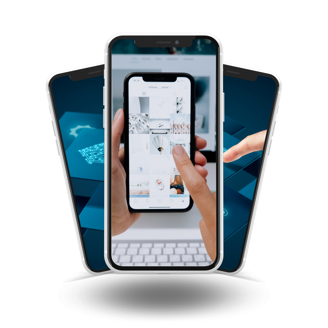
Mobile app design focuses on the visual and interactive aspects of the app, ensuring it is aesthetically pleasing and easy to navigate. Development, on the other hand, involves the technical aspects, […]
Custom software is built with flexibility and scalability in mind. It can grow with your business, adapt to changing needs, and integrate seamlessly with other systems. Additionally, custom software […]